
Physical Design Course
📅 Start Date: Coming Soon
🕒 Duration: 6 Months | Mode: Offline
🎯 Includes: 2–3 Projects + Free Internship Worth ₹8,000 + Placement Assistance
Course Fees: ₹22,000/-
📘 Course Overview
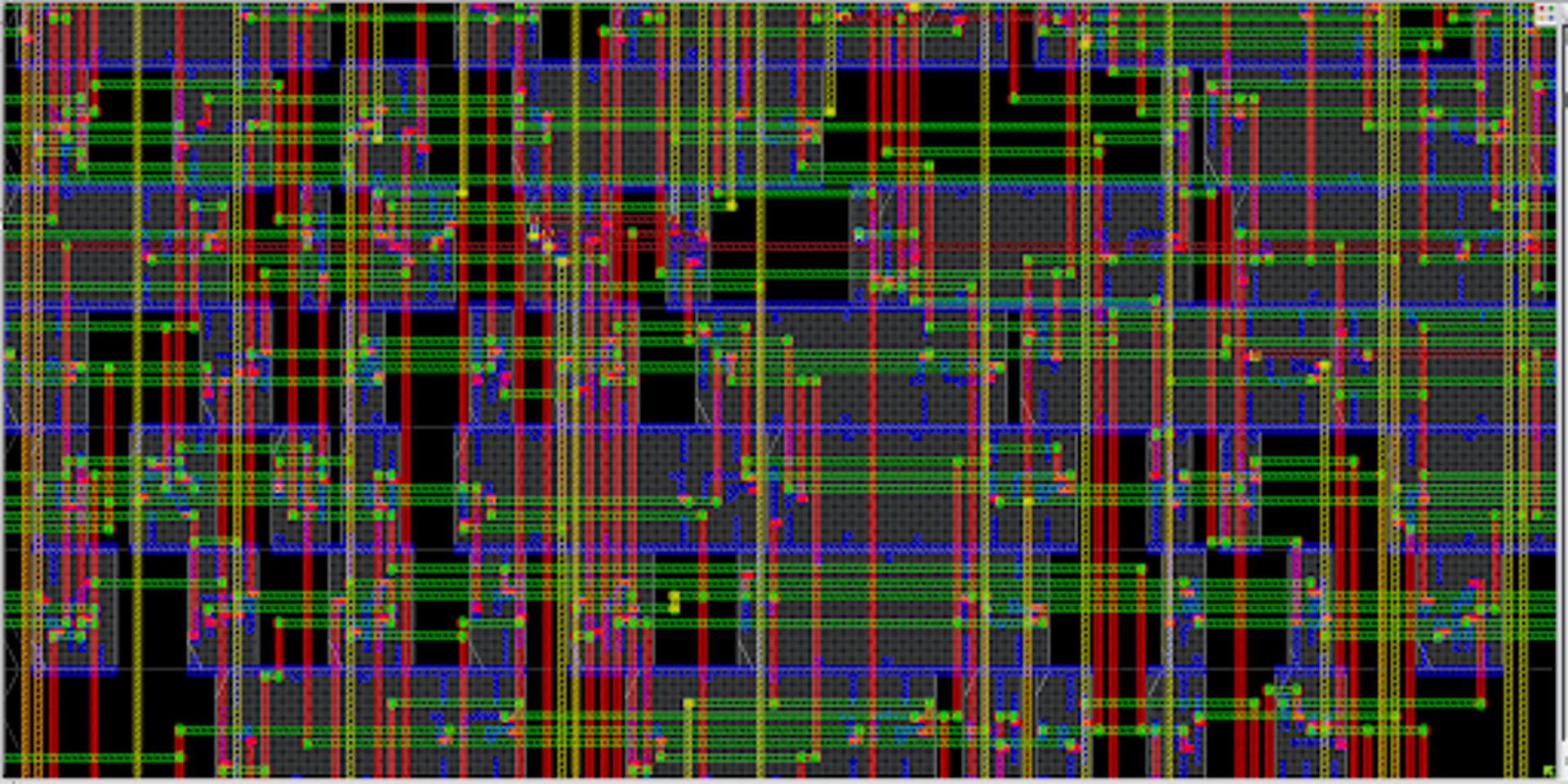
This 6-month program provides end-to-end training in ASIC Physical Design, guiding learners from synthesis to GDSII.
You’ll gain deep practical knowledge of floorplanning, placement, clock tree synthesis, routing, timing closure, and sign-off checks — using industry workflows and tools.
The course also integrates mock interviews, projects, and internship exposure to ensure you’re job-ready for back-end VLSI roles.
🗓️ Detailed Course Timeline
Month 1 – Digital Design Review & Introduction to Physical Design
Overview of ASIC Flow: Front-End vs. Back-End
RTL to GDSII Design Flow
Introduction to EDA Tools (Cadence / Synopsys / Mentor)
Design Libraries: Standard Cells, LEF/DEF Files
Understanding Netlist, Constraints, and Floorplanning Concepts
✅ Mock Interview 1: ASIC Flow and Physical Design Basics
Month 2 – Logic Synthesis & Floorplanning
Logic Synthesis using Design Compiler / Genus
Timing Constraints (SDC) and Reports
Floorplanning: Core, Die, IO, and Power Planning
Block Placement and Aspect Ratio Optimization
IR Drop and Power Grid Design
Mini Project: Basic Floorplan and Power Plan Implementation
✅ Mock Interview 2: Floorplanning and Power Planning Concepts
Month 3 – Placement & Clock Tree Synthesis (CTS)
Placement Techniques and Optimization
Congestion Analysis and Fixes
Clock Tree Synthesis (CTS): Concepts, Buffers, and Skew Optimization
Hold & Setup Time Fixes
CTS Reports and Timing Checks
Project: Placement + CTS on Standard Cell Design
✅ Mock Interview 3: Placement and CTS Design Flow
Month 4 – Routing, Timing Closure & Optimization
Routing Stages: Global and Detailed Routing
Signal Integrity and Crosstalk Analysis
Timing Closure Techniques and ECO (Engineering Change Order)
DRC and LVS Checks after Routing
Parasitic Extraction and STA Overview
Project: Complete Placement, CTS & Routing Flow
✅ Mock Interview 4: Routing, STA, and Timing Closure Concepts
Month 5 – Sign-off, Power Analysis & Tapeout
Static Timing Analysis (STA) and Sign-off Checks
Power Analysis and IR Drop Verification
Layout vs. Schematic (LVS) and DRC Closure
Tapeout Preparation and GDSII Generation
Case Study: Block-Level Chip Implementation Flow
✅ Mock Interview 5: Full Back-End Flow and Tapeout Readiness
Month 6 – Internship, Final Project & Placement Prep
Capstone Project: RTL-to-GDSII Flow for a Mini ASIC Design
Internship (Worth ₹8,000) – Work on Real Design Scenarios
Resume Building & Portfolio Guidance
Final Mock Technical + HR Interviews
✅ Mock Interview 6: Comprehensive Technical + HR Evaluation
🎓 Certification & Outcomes
Certificate of Completion
Letter of Recommendation for top performers
2–3 Industry-Grade Projects + Internship Experience
Placement Assistance for top-performing candidates
💡 Ideal For
B.E/B.Tech/M.Tech students in ECE, EEE, or Instrumentation
Fresh graduates aiming for ASIC Back-End (Physical Design) roles
Professionals seeking a complete understanding of RTL-to-GDSII flow