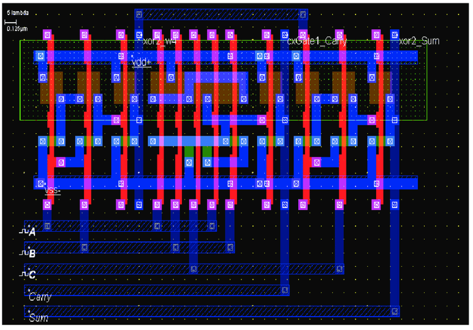
Aalog Layout Design Course
📅 Start Date: January 12, 2026
🕒 Duration: 3 Months | Mode: Online
🎯 Includes: 1–2 Projects
Course Fess: ₹6,499/-
📘 Analog Layout Design
Duration: 3 Months
Module 1: Analog IC & Layout Fundamentals
Introduction to analog integrated circuits
Role of layout in analog and mixed-signal designs
CMOS process overview (basic)
Device physics relevance to layout
MOS transistor structure and layout representation
Matching, symmetry, and layout-dependent effects
Parasitics and their impact on analog performance
Layout versus schematic correlation
Module 2: Layout Techniques for Analog Blocks
Transistor-level layout techniques
Common-centroid and interdigitated structures
Guard rings and substrate isolation
Well and substrate contacts
Routing strategies for analog signals
Power and ground routing concepts
Device sizing considerations in layout
Layout strategies for current mirrors
Layout considerations for differential pairs
Module 3: Verification, Best Practices & Capstone Project
Design rule concepts and layout constraints
Layout versus schematic (LVS) fundamentals
Parasitic awareness and extraction overview
Analog layout best practices
Matching error sources and mitigation techniques
Noise coupling and shielding concepts
Electrostatic discharge (ESD) layout awareness
Documentation and layout review methodology
Capstone Project
Layout implementation of an analog block
Adherence to matching and symmetry requirements
Verification against schematic intent
Identification and correction of layout issues
Final layout presentation and documentation
Example project domains:
Current Mirror
Differential Amplifier
Simple Operational Amplifier
Program Outcomes
Proficiency in analog layout fundamentals
Ability to implement matched and symmetric layouts
Understanding of layout-related parasitic effects
Readiness for entry-level Analog Layout roles
Post-Program Benefits
Program Completion Certificate
Capstone Project Certification
Resume Building & Profile Optimization
Mock Technical Interviews
RTL & Verification Interview Preparation
Project Review & Feedback
Career Guidance Sessions
